All Publications /
Publications:
Laser diode area melting for high speed additive manufacturing of metallic components
30 / 10 / 17
Paper: Laser diode area melting (DAM) for high speed additive manufacturing of metallic components
Publication: Materials & Design, 117, 305 (2017)
Authors: Miguel Zavala-Arredondo, Nicholas Boone, Jon Willmott, David T.D.Childs, Pavlo Ivanov, Kristian M.Groom, Kamran Mumtaz
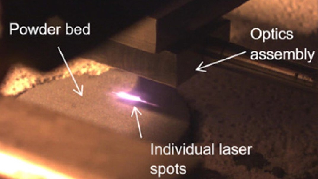
One of the challenges to the adoption of additive manufacturing (AM) in high volume sectors such as automotive is the slow speed of the process. New approaches are needed to improve process speed. The development of a new AM process - Diode Area Melting (DAM) - a highly scalable approach using energy efficient diode lasers, opens the door to faster, smaller and cheaper technologies.
The speed of typical laser AM systems is limited by the use of scanning lasers. DAM overcomes this challenge as it passes an array of individual low power laser diodes across the powder bed during production - making the system faster and more energy efficient. The paper challenges the belief that low power diode modules cannot achieve sufficient melting. Key to DAM’s success is the use of diode lasers with shorter wavelengths than typical SLM systems allowing for better energy absorption within the powder materials.
The paper can be viewed here.
More:
Publications
-
-
X1 Case Study B (UCL)
Impact of powder oxidation during additive manufacturing
Investigators: Prof Peter Lee
Researchers: Prof Chu...