All Publications /
Publications:
Additive manufacturing (AM) of energy storage devices.
03 / 03 / 20
PUBLICATION: Additive Manufacturing
AUTHORS: Fieber, L., Evans, J.D., Huang, C., Grant, P.S.
As the UK works towards its commitment to move to full electrification and zero-emissions vehicles this paper looks at additive manufacturing (AM) of
energy storage devices. The benefits of AM in terms of energy storage devices such as batteries and supercapacitors have not been widely explored.
However, this paper shows AM of supercapacitors/ EDLC’s (electro-chemical double layer capacitors) is “feasible and attractive” in some areas.
The paper demonstrates a novel, single-operation manufacturing process to fabricate fully functioning supercapacitor/EDLC devices using a hybrid AM approach.
It describes the design of a hybrid-AM system, combining low-cost fused filament fabrication (FFF) and direct ink writing (DIW) techniques.
In FFF a thermoplastic filament is liquefied by heating in a print head, extruded through a nozzle and solidified upon deposition onto a temperature controlled building platform, eventually forming the 3D part.
DIW is based on the micro-dispensing of materials as a viscous liquid ink through a small nozzle onto the building platform.
The paper states: “In the field of mass-market, ultra high area coated electrodes for conventional supercapacitor device fabrication it is unlikely that AM will be able to rival conventional
manufacturing processes in terms of economic viability, throughput and efficiency.”
It also points out that: “AM of energy storage devices may provide opportunities in new decentralized manufacturing solutions, with emphasis on material waste minimization and reduction in part specific tooling requirements.”
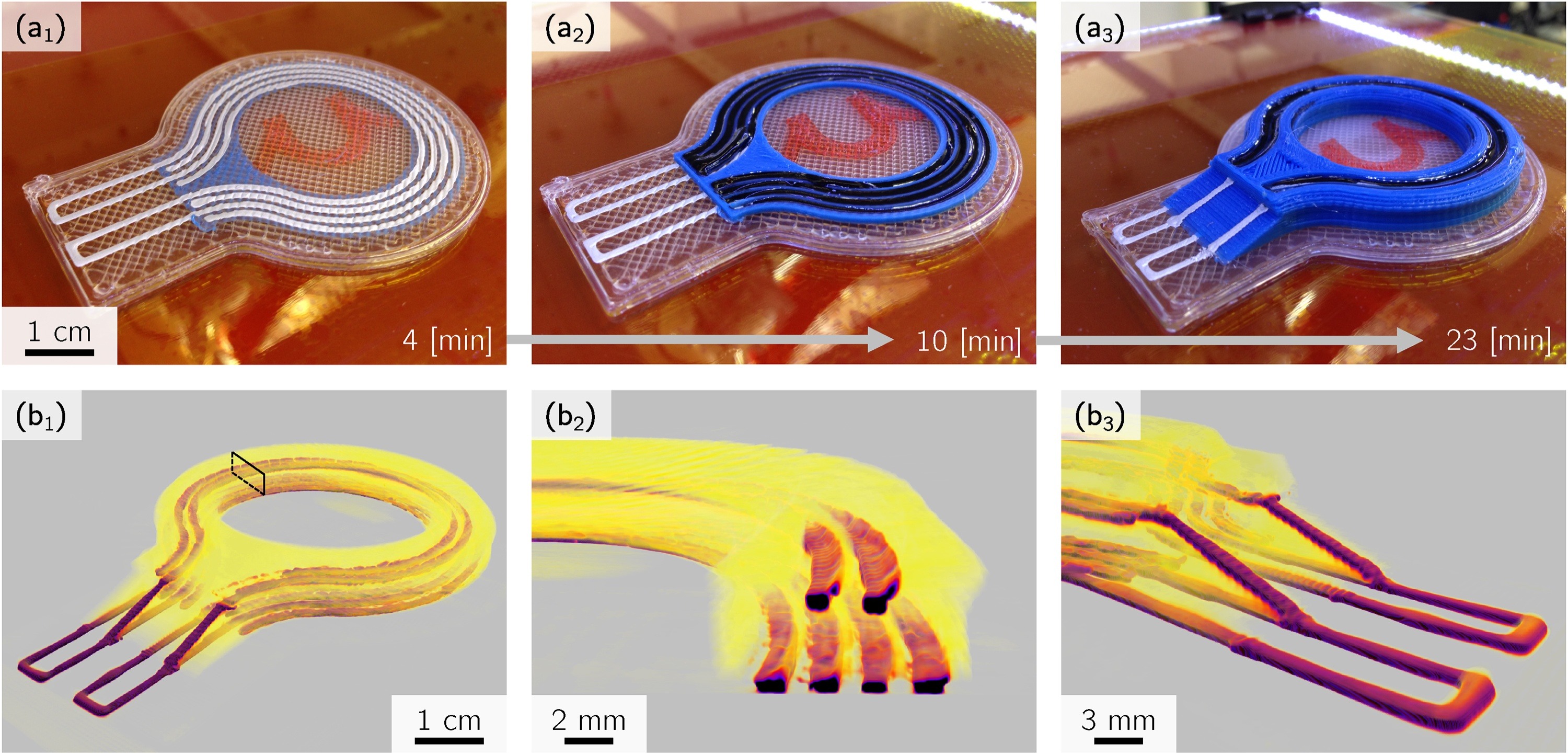
Caption:"(a) Photographs of sequential manufacture and (b) XRT renders of 3D spatial arrangement of EDLC components. (a1) Housing base layer (FFF) and current collectors (DIW), (a2) electrodes (DIW) in cavities, (a3) stacking of printed EDLCs,(b1) complete device, (b2) cross section showing stacked EDLC cells and (b3) current collector bridge
connecting stacked cells." Fieber, L., et al (2019). Attribution- NonCommercial-NoDerivatives 4.0 International licence.
More:
Publications
-
-
X1 Case Study B (UCL)
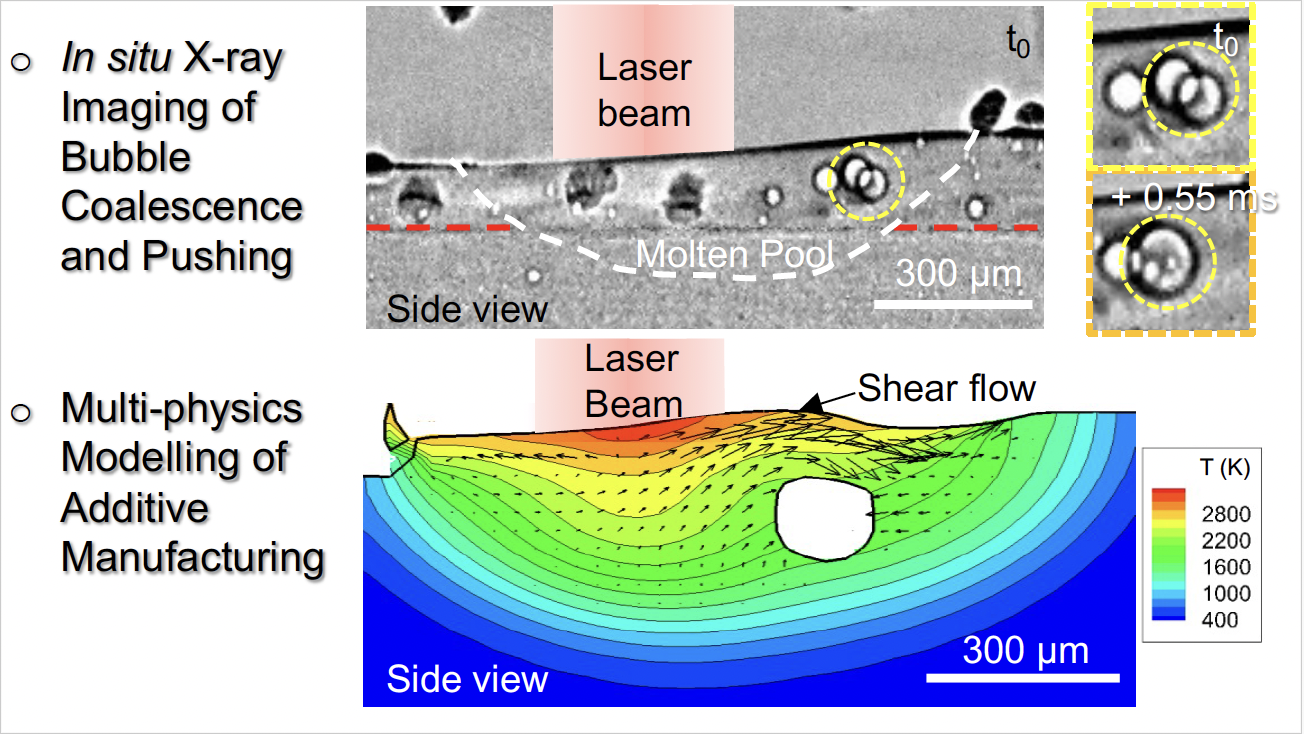
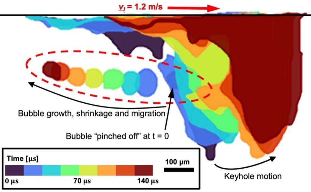
Impact of powder oxidation during additive manufacturing
Investigators: Prof Peter Lee
Researchers: Prof Chu...