All Demonstrators /
Demonstrators:
Diode Area Melting for efficient, multi-laser processing of precious and reflective metals
25 / 05 / 21
The JewelPrint project focuses on processing precious and highly challenging reflective metals using the multi-laser additive manufacturing process Diode
Area Melting (DAM).
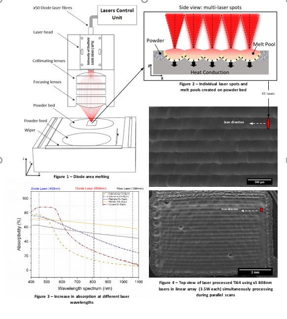
The DAM process has been developed within MAPP’s Future Manufacturing Technologies theme and uses an architectural array of low power, fibre coupled diode lasers to process pre-deposited powder (Figure 1).
Efficiently packed fibre arrays are integrated into a custom laser head designed to traverse across the powder bed. Each laser diode is individually controllable, enabling selective laser processing of powder bed cross-sections and layered fabrication of 3D net-shape components (Figure 2).
This process is inherently scalable, allowing hundreds if not thousands of lasers to simultaneously traverse and parallel scan across a build area, significantly increasing
the productivity of state-of-the-art powder bed fusion.
The Jewelprint Project, supported by Innovate UK and Diamond Centre Wales, has focused on tuning laser wavelengths to the optimum absorption profiles of precious, reflective and engineering grade alloys e.g platinum, gold, copper and titanium alloys (Figure 3).
Operating at shorter wavelengths (450-808nm) compared to traditional selective laser melting systems (1064nm), the powdered material’s ability to absorb laser energy increases, processing becomes more efficient and less laser energy is subsequently required to melt the material.
Highly reflective metals such as platinum, gold and copper were processed using individual laser powers of only 3.5W at 808nm, with further increased melt pool temperatures observed using shorter wavelength blue lasers (450nm).
Figure 4 shows the top surface profile of multiple parallel scans using x5 lasers, simultaneously scanning across a titanium alloy powder bed, creating broad melt pool tracks (250um), with components approaching 99 per cent density.
This project has shown the potential use of low power, low cost, short wavelength laser sources. Using a highly scalable methodology for the production of components from even the most reflective metals with the efficient matching of absorption profiles with laser wavelength.
More:
Demonstrators
-
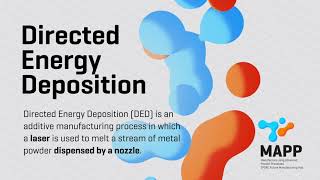
Video/ Animation illustrating Directed Energy Deposition (DED) -
Solid-State Processing of Surplus Aluminium Alloy Powders through a Combination of Field Assisted Sintering Technology and Hot Rolling
The Sheffield Titanium Alloy Research [STAR] group partners with ECKART GmbH to convert surplus aluminium alloy powders from atomisation...
-