About us / The Team / Industrial Advisory Board /
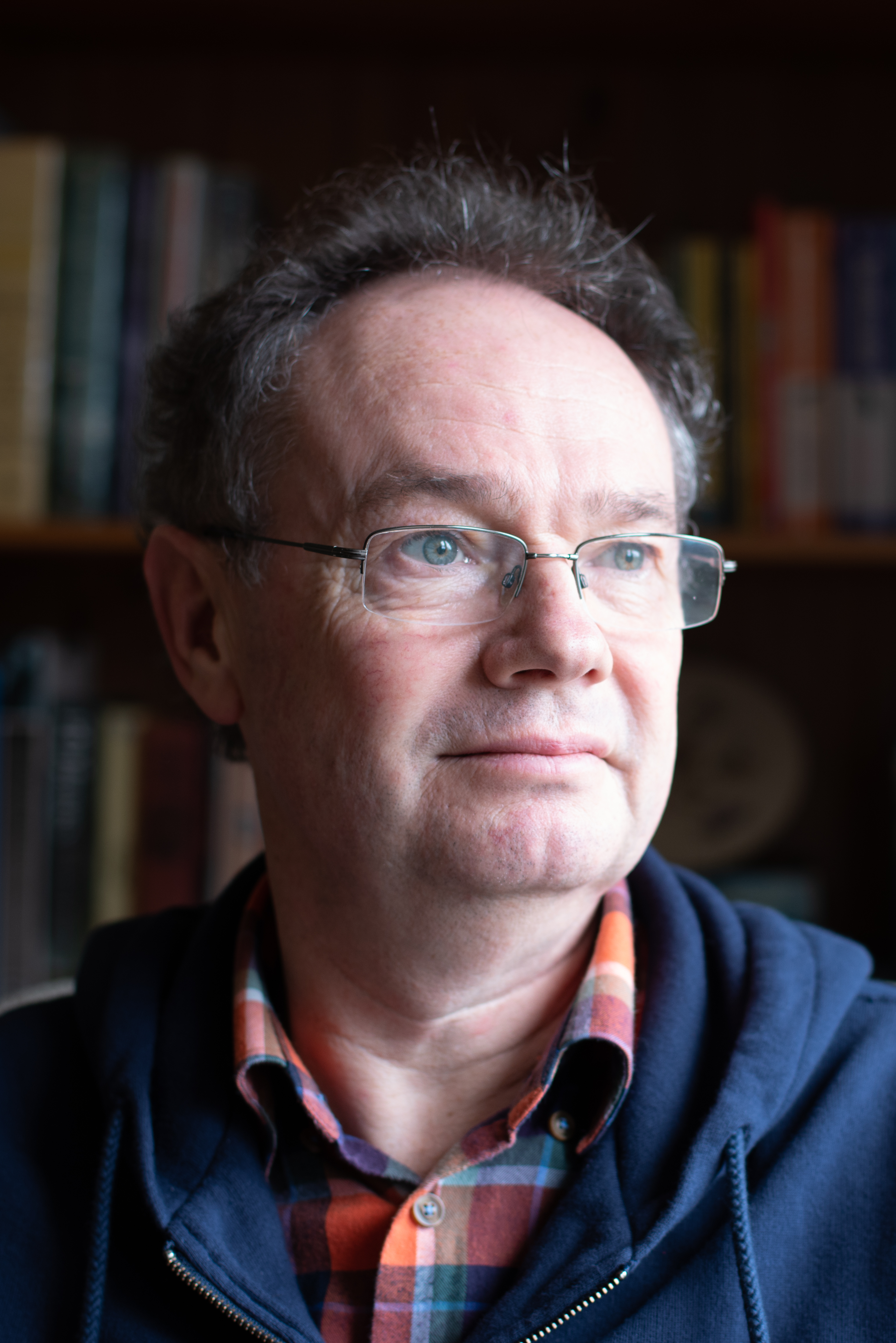
Ian Laidler
Wayland Additive
Chief Technology Officer
Ian is a physicist and engineer with 30 years of experience directing complex technical developments of high value capital equipment for the semiconductor and medical industries. Ian has worked on the introduction of a superconducting electron synchrotron for IBM’s X-ray Lithography program; superconducting proton cyclotrons for PET scanners; X-ray beamlines for the world’s third-generation synchrotrons; and electron beam lithography systems for the semiconductor and nanotechnology industries. Throughout these programs, Ian has been responsible
for coordinating high performing teams and delivering to incredibly demanding semiconductor fab environments, including customers such as IBM, Hitachi, SEAGATE, Hoya, KERI, NIST.